A Guide to High-Purity Restoration with Professional Semiconductor Cleaning
- Tech
Jessica C. Dills
- 0
- 7 minutes read
.
Key Takeaways
- Microscopic particles are the greatest threat to modern wafer fabrication and yield rates.
- Specialised semiconductor cleaning techniques preserve the delicate geometry of high-tech components.
- Regular semiconductor parts cleaning extends the operational lifespan of expensive machinery and reduces capital expenditure.
- There is a scientific difference between standard industrial washing and high-purity semiconductor restoration.
Introduction
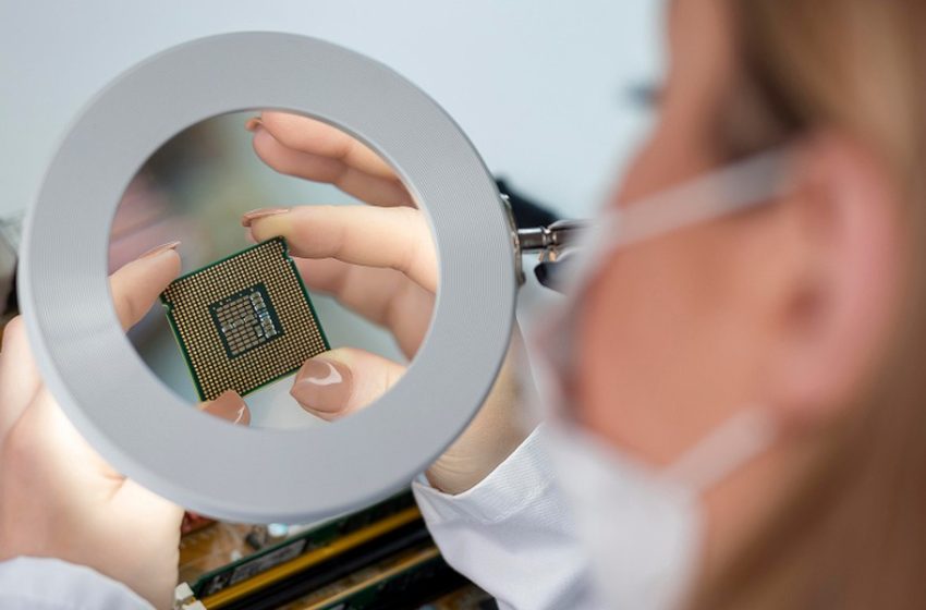
The semiconductor industry is the silent heartbeat of 21st-century civilisation. However, this industry operates on a scale so small that a single speck of dust can be as catastrophic as a boulder falling onto a glass house. In the high-stakes environment of a cleanroom, the margin for error is nonexistent. Achieving the perfect percentage of functional chips produced is a constant battle against the invisible forces of contamination. The intricate world of semiconductor cleaning maintains a pristine manufacturing environment, and the technical nuances ensure every component performs at its peak.
The Atomic Impact of Ionic and Metallic Residues
If a machine looks polished and free of grease, it is considered ready for use. In the world of microelectronics, however, contaminants come in various forms: ionic particles, organic residues, and metallic impurities. Each of these can interfere with the atomic-level pathways of a microchip. This is why semiconductor cleaning is a critical step in the manufacturing workflow. It requires an understanding of molecular chemistry and fluid dynamics to ensure that even the most stubborn residues are lifted without etching or damaging the substrate itself.
Addressing the Shadowing Effects of High-Aspect Ratios
The complexity of modern chip architecture means that the aspect ratio of the parts involved is incredibly high. Narrow trenches and deep holes act as traps for particulates. Traditional cleaning methods often fail to penetrate these tiny crevices. Professional decontamination services utilise advanced surfactants and precision-agitated baths to ensure that every surface, no matter how obscured, is reached. This level of detail is what separates a world-class fabrication plant from one plagued by frequent downtime and poor product reliability.
Preventing Flake-Off in CVD and Etching Tools
The equipment used to create them is equally susceptible to the ravages of the production process. Chemical Vapour Deposition (CVD) and etching tools frequently accumulate by-product buildup on their internal chambers and shields. If left unaddressed, these deposits can flake off during the next production cycle, landing on a fresh wafer and ruining thousands of dollars’ worth of product. Semiconductor parts cleaning involves the removal and deep-cleaning of specialised components.
Material-Specific Protocols for Tool Components
The technical challenge in semiconductor parts cleaning lies in the diversity of materials used. A single tool might contain parts made of quartz, ceramic, stainless steel, and various high-performance polymers. A chemical that effectively removes a polymer residue might inadvertently corrode a ceramic coating. By maintaining a strict schedule for part restoration, manufacturers can significantly extend the time between major tool overhauls, boosting overall factory efficiency.
The Risks of Surface Roughening through Over-Cleaning
Excessive exposure to harsh acids or bases can lead to surface roughening, which actually creates more surface area for future contaminants to latch onto. Professional restoration is about using the minimum chemical and mechanical force necessary to achieve the required purity level. This nuance preserves the dimensional tolerances of the parts, ensuring they fit perfectly back into the machine and function with the precision required for high-frequency microelectronics fabrication.
The Financial Benefits of Restoration over Replacement
When a major contamination event occurs, the immediate instinct might be to replace all affected equipment. Lead times for new tools can stretch into years, and the capital expenditure involved is astronomical. Professional industrial decontamination, particularly specialised semiconductor cleaning, offers a viable middle ground. Experts can determine the exact level of contamination and develop a targeted restoration plan.
Predictive Maintenance as Insurance against Downtime
Regular semiconductor parts cleaning allows for the early detection of wear and tear, such as micro-cracking or coating depletion. Identifying these issues during a scheduled clean is far less disruptive than a sudden tool failure in the middle of a high-priority production run. In this sense, professional cleaning provides the data and the physical assurance needed to run a facility at maximum capacity with minimal risk. The precision of your cleaning partner is often the deciding factor in your competitive edge.
Conclusion
The role of contamination control will only grow in importance. Semiconductor cleaning is a fundamental pillar of modern engineering that ensures the reliability of our most advanced technologies. Through the meticulous process of semiconductor parts cleaning, we protect the massive investments made in fabrication machinery and ensure that yield rates remain high. Purity is a goal and a discipline. When you master that discipline, you unlock the full potential of the silicon age, creating a world where technology is smaller, faster, and more reliable than ever before.
Is invisible contamination eating away at your yield rates? Reach out to BELFOR Singapore and discover precision cleaning secrets today.